How Wide-Bandgap Semiconductors Improve Transformer Efficiency
Wide-bandgap semiconductors help solid-state transformers waste less power, run at much higher switching speeds, and use much smaller magnetics. In plain terms: SiC and GaN cut switching loss, which lets SSTs move from bulky 60 Hz iron-core designs to compact systems with 5 kHz to 100 kHz medium-frequency transformers. That can mean 25% to 40% lower conversion losses than silicon-based devices in some designs, plus up to 50% less cooling system size.
If I had to sum up the article in a few lines, it would be this:
- SiC MOSFETs fit the medium-voltage side of an SST, where voltage ratings like 13.2 kV and 34.5 kV matter.
- GaN HEMTs fit the low-voltage side, where very high switching speed matters more than top-end voltage blocking.
- The main SST losses show up in the AC-DC stage, isolated DC-DC stage, and DC-AC stage - with the isolated DC-DC section often taking the biggest hit.
- Higher switching frequency shrinks the transformer, copper, and some cooling hardware, but it also makes insulation, EMI, thermal control, and protection settings harder to deal with.
- The tradeoff is simple: better efficiency, smaller size, and more control in exchange for more design work and a price that can be about 2x a standard transformer.
Here’s the short version of what matters most to you:
| Topic | What the article says |
|---|---|
| Main efficiency driver | Lower switching and conduction losses from SiC and GaN |
| Why SSTs are smaller | They use a medium-frequency transformer instead of a 60 Hz core |
| Best use of SiC | MV input stages and the main power path |
| Best use of GaN | LV output stages with very fast switching |
| Typical gain figures | 25%–40% lower conversion losses, 99% conversion efficiency in some SiC SST designs |
| Main design problems | Insulation stress, partial discharge risk, cooling, gate drive limits, relay changes |
| Main cost issue | Around 2x the upfront cost of a line-frequency transformer |
The bottom line: WBG devices make SSTs smaller, cooler, and more efficient because they switch faster with less loss. But if I’m specifying one for a U.S. site, I also need to check feeder voltage, switchgear, insulation, fault behavior, and cooling support before the efficiency numbers mean much in practice.
Tech Bytes Ep 1: Solid State Transformers (SSTs) | Smart Grid Revolution
sbb-itb-501186b
Where Losses Occur in Solid-State Transformer Designs
An SST has three conversion stages, and each one adds its own losses. That’s the core design tradeoff: every stage solves one problem while creating another. Once you see where the losses show up, it becomes much easier to judge which devices, switching frequencies, and magnetic parts make sense next.
Main Loss Sources in Each SST Stage
The main loss sources by stage are shown below.
| SST Stage | Primary Components | Key Loss Sources |
|---|---|---|
| AC-DC Front End | PWM Rectifier, SiC MOSFETs | Conduction loss, switching loss, EMI filter loss |
| Isolated DC-DC | Dual Active Bridge (DAB), MFT | MFT core (hysteresis/eddy-current) and copper losses, high-frequency switching losses |
| DC-AC Output | Inverter, LV DC Link | Conduction loss, auxiliary and control power |
In most cases, the isolated DC-DC stage is where the biggest loss shows up. This stage uses a Dual Active Bridge (DAB) and a medium-frequency transformer (MFT), so the loss doesn’t come from just one place. It comes from semiconductor switching, transformer core losses, and copper or winding losses.
This is exactly where WBG devices start to matter. They let designers switch at higher frequencies while cutting loss during each switching event. But there’s no free lunch. Push frequency up, and more loss moves into the semiconductors. Keep frequency lower, and the transformer gets larger, with more copper loss to deal with. That’s why material choice matters too. Nanocrystalline cores help keep high-frequency core loss under control.
Cooling tells part of the story as well. In commercial MV-SSTs, the cooling system is often the largest subsystem, which makes it a pretty blunt signal of how much loss is still left in the design.
Why Conventional Silicon Creates Design Limits
Conventional silicon puts a hard cap on SST efficiency because it slows switching and brings more heat with it. Standard 6,500 V silicon IGBTs are generally limited to switching frequencies of a few hundred hertz, since switching losses climb fast as frequency rises.
That limit has a domino effect. If switching frequency stays low, designers are pushed toward large, heavy iron-core magnetics and thicker copper windings. The system works, but it loses the size and weight gains that make SSTs appealing in the first place.
Silicon-steel cores make this even tougher. They are generally limited to about 1 kHz because eddy-current and hysteresis losses become excessive. So instead of using compact medium-frequency transformers, silicon-based SST designs end up leaning on bulky magnetic parts.
There’s also reverse recovery to deal with. Silicon devices have higher reverse recovery-related losses than SiC, which adds more heat during switching transitions.
That loss map shapes the device and topology choices in the next stage of design.
How SiC and GaN Reduce Losses and Increase Power Density
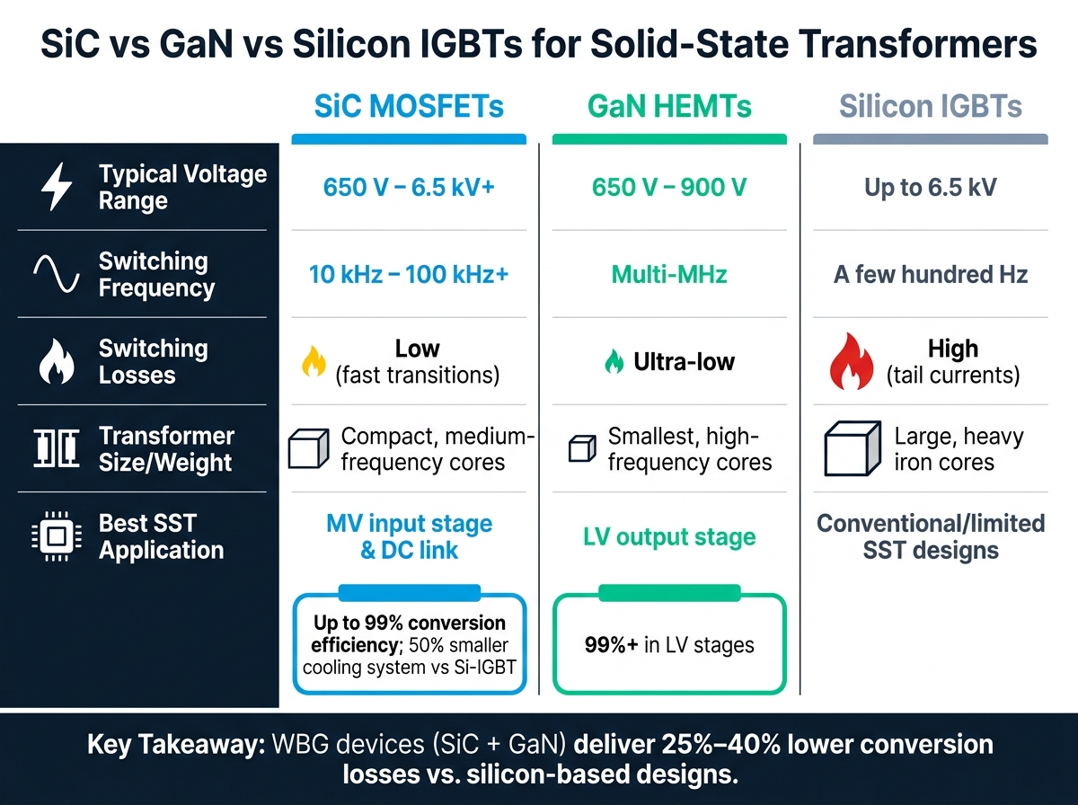
SiC vs GaN vs Silicon IGBTs for Solid-State Transformers
Once you know where the losses come from, the next step is simple: figure out which WBG device cuts them best.
Lower Conduction and Switching Losses with WBG Devices
SiC MOSFETs trim the switching and conduction losses that hit hardest in the AC-DC and DC-DC stages. Silicon IGBTs have a well-known problem during turn-off: tail currents. Those currents keep flowing for a short time and dump energy into heat on every switching cycle. SiC sidesteps that issue, so each cycle wastes less energy and the cooling system has less work to do.
The performance data lines up with that. Wolfspeed's 10 kV SiC MOSFET, CPM3-10000-0300A, showed 99% conversion efficiency in SST designs and made it possible to cut thermal cooling system size by 50% compared with standard Si-IGBT designs. GaN plays a different role. It fits the low-voltage output stage, where multi-megahertz switching matters more than high voltage blocking capability.
SiC also has another edge: it can run at high junction temperatures by design.
Higher switching speed sounds great on paper. But it only pays off if the magnetics get smaller too.
How Higher Switching Frequency Reduces Transformer Size and Copper Use
As switching frequency goes up, the core and windings needed for the same power go down. That's a big deal in SST design. Silicon IGBTs are usually stuck at a few hundred hertz because their switching losses climb too fast, which leaves designers with large, heavy iron-core transformers. SiC MOSFETs change that by pushing usable switching frequencies past 10,000 Hz, which makes compact medium-frequency transformers, or MFTs, a practical option. GaN goes even further in low-voltage stages, into the multi-megahertz range, which shrinks magnetics even more in those use cases.
"Higher switching frequency in SSTs directly reduces the size and weight of the magnetic components, because the required magnetic coils and core size decrease as frequency increases."
- Ashish Kumar, Ph.D., MVHV Research Scientist, Wolfspeed
There is a trade-off. Higher frequency calls for tighter insulation coordination. A Georgia Tech 2021 prototype handled this with nanocrystalline cores and 15 kV-rated insulation.
The table below shows how these device types line up in SST use.
Comparison Table: Silicon IGBTs vs. SiC MOSFETs vs. GaN for SST Applications
| Feature | Silicon IGBTs | SiC MOSFETs | GaN HEMTs |
|---|---|---|---|
| Typical Voltage Range | Up to 6.5 kV | 650 V – 6.5 kV+ | 650 V – 900 V |
| Switching Frequency | A few hundred Hz | 10 kHz – 100 kHz+ | Multi-MHz |
| Switching Losses | High (tail currents) | Low (fast transitions) | Ultra-low |
| Transformer Size/Weight | Large, heavy iron cores | Compact, medium-frequency cores | Smallest, high-frequency cores |
| Best SST Application | Conventional/limited SST designs | MV input stage & DC link | LV output stage |
In practice, that split is pretty clean. SiC works best in the medium-voltage stages, while GaN makes more sense in the low-voltage output stage. A hybrid setup lets designers use the strong points of both without forcing either one beyond its dependable operating range.
How to Design or Specify a WBG-Based Transformer System
Choosing the Right WBG Device and Converter Topology
Start with two things: your efficiency target and your voltage class. That narrows the device choice fast.
SiC MOSFETs are a good fit for medium-voltage interfaces, covering 4.16 kV and 13.8 kV systems with 3.3 kV to 6.5 kV devices. GaN fits low-voltage output stages and high-frequency rack conversion. After that, topology does the heavy lifting. It decides how voltage moves through the system and how much loss you can cut along the way.
For the MV grid interface, use MMC or cascaded H-bridge topologies. For isolated DC-DC conversion, use a DAB. Below 5 kV, series-stacked multilevel architectures make sense. Around 10 kV, a simpler two-level cell starts to look practical. One catch: commercial 10 kV gate drivers are still limited, so custom development may be needed.
Delta’s 13.8 kV, 400 kW charger is a good proof point. It reached 96.5% efficiency without a low-frequency transformer. Once the converter path is set, the next job is harder than it sounds: magnetics, insulation, and cooling all need to be reworked for higher switching speeds.
Redesigning Magnetics, Insulation, and Cooling for Higher Switching Speeds
At 10–30 kHz, nanocrystalline cores and Litz wire help keep core, skin, and proximity losses in check. Push switching frequency up, and the magnetics get smaller. That's the upside. The trade-off is that insulation and thermal design get tougher.
Higher dv/dt changes transformer design in a direct way. It doesn't just affect switching behavior. It also pushes up partial-discharge risk, which means medium-voltage SSTs need much more insulation margin. In one example, a 35 kV design can need roughly 100 kV of insulation on the high-frequency transformer. Materials such as silicon nitride or aluminum nitride can help handle higher electric field strengths.
Standards are still catching up here. IEEE, IEC, and UL guidance for insulation coordination in high-frequency WBG systems is still changing, so design reviews should stay tied to the latest updates.
Heat is another sticking point. The remaining loss is concentrated at the die, so high-conductivity thermal interface materials and heat spreaders matter a lot. For high-power-density SSTs, liquid cooling is the practical option. Diamond or AlN can help pull heat away from tight hot spots. Forced-air cooling can still work at lower power levels, but it's smart to check site cooling support early. A lot of projects come down to one simple question: can the facility support a liquid loop?
Those hardware decisions shape the thermal and cost trade-offs that come next.
Design Trade-Off Table: Efficiency, Size, Complexity, and Cost
| Design Variable | Choice | Efficiency Impact | Size/Weight Impact | Complexity |
|---|---|---|---|---|
| Device (MV stage) | SiC MOSFET | High (98%–99%) | 70%–80% reduction vs. LFT | Medium–High |
| Device (LV stage) | GaN HEMT | Very high (99%+) | Maximum compactness | Medium |
| Switching frequency | 10–100 kHz (SiC) | Improves with frequency | Significant reduction | Increases with frequency |
| Topology (DC-DC) | Dual-Active Bridge | Used for isolated conversion | Compact | Medium |
| Topology (AC-DC) | Modular Multilevel | Scalable to MV grids | Modular, serviceable | High |
SSTs are currently about 2x the price of conventional line-frequency transformers.
Implementation, Equipment Planning, and Key Takeaways
Integrating WBG-Based SSTs with Existing U.S. Distribution Equipment
Once the device is chosen, the next step is integration. This is where the project gets very practical, very fast.
A WBG-based SST retrofit only works if the rest of the distribution setup can support it. Before commissioning, teams need to check feeder voltage, switchgear, protection, and cooling compatibility.
In the U.S., distribution feeders usually operate from 13.2 kV to 35 kV. In many retrofit cases, the main constraint is MFT insulation.
Fault behavior also changes. SSTs can limit fault current to about 1.5x nominal, which sounds helpful - and it is - but protection settings still need a full review. Relay coordination and DC fault-clearing settings must be redesigned to fit the new system behavior.
If a full swap isn’t realistic, a Hybrid SST can offer a middle ground. It creates a retrofit path by pairing an SST stage with a conventional dry-type transformer.
That’s why procurement can’t wait until the last minute. Teams should line up compatible breakers, switchgear, and existing distribution gear early, before those parts turn into schedule problems.
Compatibility and Upgrade Planning Table for Retrofit Projects
These interface checks help decide whether the efficiency gains from WBG devices will hold up outside the lab and in day-to-day operation.
| Existing Equipment | Required SST Interface / Upgrade | Efficiency Impact | Installation Notes |
|---|---|---|---|
| Legacy oil-filled transformers | Full replacement with SST or Hybrid SST | Can improve overall efficiency in retrofit applications | Verify code compliance and utility interconnection requirements |
| Low-voltage switchgear | Integration with 800 VDC busbars; DC-rated breakers required | Reduces copper use at higher DC voltage | Confirm DC interrupting ratings and compatibility with the selected DC architecture |
| Protection devices (relays, breakers) | Reconfigure for controllable fault current and updated relay coordination | Minimal direct efficiency impact | Coordinate fast DC fault clearing with existing protection settings |
| Cooling systems | Can be downsized; SiC-based SSTs can reduce thermal cooling requirements | Reduces auxiliary power draw | Evaluate forced-air, deionized-water, or dielectric-fluid cooling based on facility constraints |
Conclusion: Key Reasons WBG Devices Raise SST Efficiency
WBG devices improve SST efficiency by cutting switching loss, shrinking magnetics, and lowering cooling demand.
But that gain doesn’t happen by default. It depends on choosing the right device and matching it to the converter topology, insulation limits, thermal setup, and target voltage class.
FAQs
Why are SiC and GaN used in different SST stages?
SiC and GaN tend to show up in different solid-state transformer stages for a simple reason: they’re built for different jobs.
SiC MOSFETs are a good fit for medium-voltage input stages and DC links, where high-voltage strength and strong thermal behavior matter most. GaN, by contrast, is more common in low-voltage output stages, where its lateral structure allows very high switching frequencies.
What limits switching frequency in SSTs?
Switching frequency in solid-state transformers is mostly held back by two things: the magnetic material inside the high-frequency transformer and the switching losses in the power semiconductors.
Conventional silicon-steel cores stop working well above 1 kHz. The main reason is higher eddy-current and hysteresis losses. Once frequency climbs, those losses add up fast.
Newer materials, such as nanocrystalline alloys, can handle about 5 to 100 kHz. That opens the door to much higher-frequency operation. But there’s a catch: as frequency goes up, dielectric losses and switching losses go up too. More loss means more heat, and more heat means tougher thermal management.
Are SST retrofits practical for existing U.S. systems?
Yes - SST retrofits are becoming more practical in U.S. systems, especially in places where space is tight and power quality is a big concern. They can also ease pressure when lead times for standard transformers stretch out.
The upfront price is still higher. But over time, SSTs can help cut costs through better efficiency, active voltage regulation, a smaller footprint, and direct DC output for modern loads.