5 Methods to Reduce Noise in Voltage Regulators
If you want a cleaner power rail, I’d start with layout and decoupling first, then add filtering, a low-noise LDO, or a post-regulator only if the noise target still isn’t met.
Here’s the short version: regulator noise usually comes from switching ripple, internal LDO noise, weak decoupling, PCB parasitics, and load transients. And one point matters a lot: PSRR drops at high frequency, so a regulator that blocks noise well at low frequency may do much less above 1 MHz.
If I had to boil the article down, these are the 5 methods:
- Add output capacitors to shunt high-frequency ripple and spikes
- Use an LC or pi filter when capacitors alone don’t cut switching noise
- Fix PCB layout and switching loops to reduce ringing, overshoot, and EMI pickup
- Pick a low-noise LDO for rails that feed ADCs, DACs, PLLs, VCOs, and clocks
- Add an NR network or post-regulator stage for the last bit of cleanup
A few numbers stand out:
- 60 dB PSRR means about 1,000x noise reduction at that test point
- LC and pi filters help most in the 500 kHz to 3 MHz range
- An NR network example cut LDO noise from 70 µV RMS to 12 µV RMS
- But a 1 µF NR capacitor stretched startup from 600 µs to 600 ms
- A second LDO stage can cut ripple by 10x or more
How to Reduce Power Regulator Switching Noise | Schematic Capture
sbb-itb-501186b
Quick comparison
| Method | What I’d use it for | Main tradeoff |
|---|---|---|
| Output capacitors | High-frequency ripple at the load | Wrong type or poor placement limits results |
| LC / pi filter | Switching noise and edge spikes | Can ring and takes more board space |
| PCB layout | Noise caused by loops, parasitics, and bad returns | Needs board-level rework |
| Low-noise LDO | Cleaning sensitive analog or RF rails | Costs dropout headroom |
| NR network / post-regulator | Last-stage noise cleanup | Slower startup or more voltage loss |
The main idea is simple: match the fix to the noise source. If noise is getting in through layout, more capacitors won’t solve much. If the rail feeds a sensitive ADC or PLL, a low-noise post stage may be the better move.
What Causes Noise in Voltage Regulators
Voltage regulator noise doesn't come from just one place. It usually comes from a few different spots, and the right fix depends on which one is doing most of the damage.
Switching regulators tend to add ripple and spikes. Linear regulators, including LDOs, tend to add internal reference noise and error amplifier noise.
Decoupling can make or break the result. If it's weak, noise gets worse fast. Capacitors aren't ideal parts, after all. They come with ESR and ESL, and high ESL hurts high-frequency filtering, which lets more noise slip through.
PCB layout is another big one. Trace inductance can lead to ringing and overshoot. Longer traces can also act like little antennas and pick up noise from nearby switching nodes. That's why a short, continuous ground return path matters so much. It helps cut loop inductance.
Load transients add their own mess. Sudden current changes can cause voltage dips, ringing, or even instability, especially when undamped LC filters are involved.
When you measure this stuff, the unit matters. Use mV p-p for ripple and spikes. Use µV RMS for random noise, usually integrated from 10 Hz to 100 kHz. And for Gaussian white noise, the RMS value is roughly 1/6 of the peak-to-peak value.
The table below shows the main noise sources and how they usually appear.
| Noise Source | Primary Cause | Measurement Unit |
|---|---|---|
| Switching ripple and spikes | Switching activity | mV peak-to-peak |
| Internal LDO noise | Reference and error amplifier | µV RMS (10 Hz–100 kHz) |
| Weak decoupling | High ESL/ESR in capacitors | mV peak-to-peak |
| PCB parasitics | Trace inductance, poor layout | mV or µV |
| Load transients | Sudden current changes | mV peak |
These noise sources line up directly with the five methods below.
1. Add Output Filtering Capacitors
For high-frequency ripple and spikes, output capacitors are your first line of defense. They cut output impedance and divert high-frequency noise before it gets to the load. This matters most once loop gain has fallen below 1, which is usually above 1 MHz.
At high frequencies, the output capacitor does most of the filtering.
The capacitor type matters just as much as the capacitance value. Ceramic surface-mount capacitors keep ESR and ESL low, which makes them a strong fit for high-frequency filtering. A 10-µF ceramic can have lower impedance at 1 MHz than a much larger electrolytic because it has less parasitic inductance and a higher self-resonant frequency.
That said, lower ESR and ESL aren't always a free win. Very low ESR can destabilize supplies that depend on capacitor ESR as part of the feedback network.
Capacitance size also affects startup. Large capacitance slows startup, which can be a problem in power-cycled systems. And placement matters just as much as part choice: put the capacitor at the load's power pins, not only at the regulator output.
2. Use a Pi Filter or LC Filter
An LC filter uses a series inductor and an output capacitor to create a two-pole low-pass response. A pi filter adds another capacitor before the inductor. Use one when output capacitors by themselves don't cut switching noise enough.
These filters work well for reducing switching-frequency noise in the 500 kHz to 3 MHz range, along with high-frequency switching edge noise from 50 MHz to 200 MHz.
There’s a catch: size and stability. An LC filter has a natural resonant frequency, which can lead to ringing or instability after a load transient. It also adds at least two parts, or three with a pi filter, so it takes up more PCB space.
Placement matters just as much as the parts you choose. Put the filter at the node that creates the noise:
- Use output-side filtering for boost and flyback stages
- Use input-side filtering for buck regulators, where input current is more discontinuous
This approach fits parts that are extra sensitive to rail noise, like high-resolution ADCs and DACs, low-noise op-amps, and RF PLL/VCO rails.
3. Improve PCB Layout and Switching-Loop Control
Before you add extra parts, inspect the board layout first. A small switching loop helps cut ringing, overshoot, and EMI. And if filtering doesn't solve the problem, layout is usually the next fix with the biggest payoff.
Start by finding the critical current paths. Then place parts and copper so high-current switching stays away from the control loop. This matters more than it may seem. Gate-driver paths can carry amp-level pulses in nanoseconds, so even short traces need careful routing.
For better control accuracy, keep noisy power returns out of the feedback path. A common way to do that is to use separate AGND and PGND domains, then connect them at one point near the output-capacitor return.
Keep these parts on AGND:
- Feedback dividers
- Compensation parts
- Soft-start capacitors
Keep these on PGND:
- The switch node
- Power switches
- Input and output capacitors
The SW node is the noisiest node on the board. Keep it compact, but also wide. Route current-sense lines with Kelvin connections, and if you have to use vias on gate-driver connections, use two vias per connection.
4. Choose a Low-Noise Regulator or LDO
If filtering and layout still leave too much noise, shift the fix to the regulator itself. In that case, a low-noise LDO is often the next step.
A low-noise LDO reduces internal reference noise and helps cut input ripple. But there’s a catch: PSRR drops as frequency goes up, so the gain is strongest at lower frequencies.
One detail that trips people up: adjustable LDOs can show more output noise as you set them to higher voltages. Fixed-output parts don’t have that same scaling issue.
This approach fits best on rails that feed noise-sensitive parts, such as:
- RF synthesizers
- PLLs/VCOs
- High-speed ADCs/DACs
- Clock rails
If the LDO includes an NR or bypass pin, add the recommended capacitor. That can lower low-frequency noise, though startup will usually slow down. If that still doesn’t get you where you need to be, add a noise-reduction network or use a post-regulator stage.
5. Add a Noise-Reduction Network or Post-Regulator Stage
If a low-noise LDO still leaves too much rail noise, this is the last cleanup step. In plain English, these are the end-stage fixes when filtering, layout, and a low-noise LDO still leave noise on the rail.
An NR network is a simple RC circuit added to the feedback node of an adjustable LDO. The goal is to keep AC loop gain near unity so the LDO doesn’t amplify its own internal noise. On the ADP7142 LDO, testing showed that an NR network cut measured RMS noise from 70 µV to 12 µV.
That’s a big drop. But there’s a catch: startup time can get much longer. A 1 µF NR capacitor can stretch startup from 600 µs to 600 ms. So if your system power cycles a lot, large NR capacitors can become a headache fast.
A post-regulator stage takes a different path. You place a second low-noise LDO after the main regulator to add another PSRR stage. This can cut output ripple by 10x or more. The downside is pretty simple: you lose some headroom to dropout in the second LDO, and you need more board space for the extra IC plus its input and output capacitors.
"A good, but expensive, way to reduce power-supply noise is to put a second low-noise regulator on the power-supply output... It will reduce any output ripple by an order of magnitude or more."
For the leftover high-frequency noise, pair the post-regulator LDO with a small LC or RC filter. Think of it like a two-step cleanup: the LDO handles the lower-frequency junk, while the filter helps mop up the faster noise that slips through.
| Feature | NR Network | Post-Regulator (LDO) |
|---|---|---|
| Best Frequency Range | 20 Hz – 10 kHz, sometimes up to 50 kHz | Low to mid frequency |
| Board Space | Very low (1 resistor, 1 capacitor) | Moderate to high (IC + capacitors) |
| Dropout | Negligible | 100–500 mV typical |
| Startup Time Impact | Can increase by up to 1,000x | Minimal |
| Best For | Adjustable LDOs with an accessible feedback node | ADCs, DACs, VCOs, PLLs, high-speed clocks |
Comparison Table
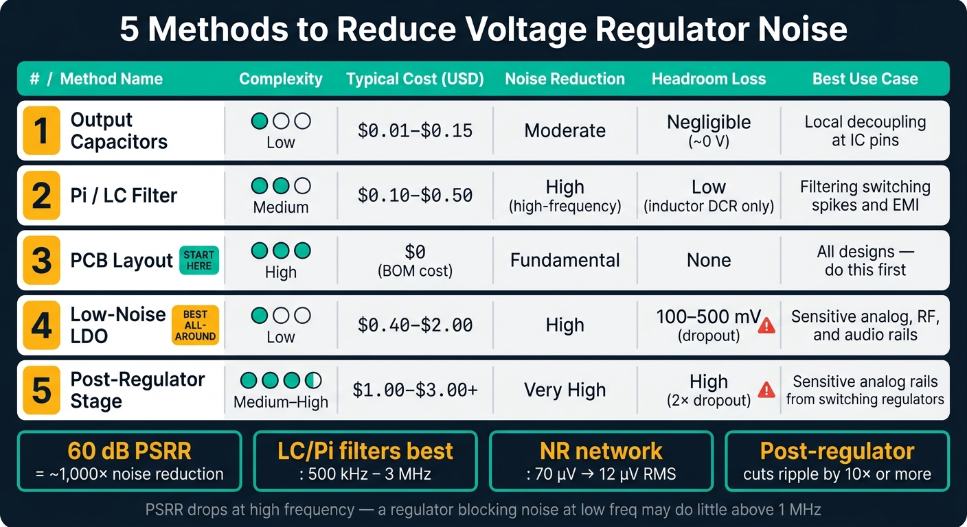
5 Methods to Reduce Voltage Regulator Noise: Quick Comparison
Use this table to line up each method with the kind of noise you're dealing with, the headroom you have, and how much room is left in your BOM budget.
| Method | Complexity | Typical Cost (USD) | Noise Reduction | Headroom Loss | Best Use Case |
|---|---|---|---|---|---|
| 1. Output Capacitors | Low | $0.01–$0.15 per unit | Moderate | Negligible (~0 V) | Local decoupling at IC pins |
| 2. Pi / LC Filter | Medium | $0.10–$0.50 | High (high-frequency) | Low (inductor DCR only) | Filtering switching spikes and EMI |
| 3. PCB Layout | High | $0 (BOM cost) | Fundamental | None | All designs |
| 4. Low-Noise LDO | Low | $0.40–$2.00 | High | 100–500 mV (dropout) | Sensitive analog, RF, and audio rails |
| 5. Post-Regulator Stage | Medium–High | $1.00–$3.00+ | Very High | High (2× dropout) | Sensitive analog rails fed from switching regulators |
Method 4 is usually the best all-around pick if you can spare the dropout headroom. It gives strong noise cleanup without adding much design hassle.
For high-current rails, don't use the RC-filter version of Method 2. That route can burn too much voltage and waste power. An LC filter or ferrite bead is the better fit.
Once you've chosen a method, the next step is to look at the common mistakes that can wipe out most of the gain.
Common Mistakes That Limit Noise Reduction
Even the best filter or regulator can fall short if the PCB layout puts noise back into the system. That’s where things often go sideways. These are the mistakes that stop the five methods from doing their job.
- Capacitors placed too far from the IC's power pins hurt Method 1. Long traces add inductance, which weakens high-frequency bypassing.
- High-current switching loops routed near FB or compensation traces hurt Methods 2 and 3. Big loops can radiate and pick up noise, then feed it straight into the control loop. Keep switching paths away from FB and compensation nodes to help keep that noise out.
- Misplaced bulk capacitors hurt Method 3. Bad placement can increase loop inductance and ground bounce. Breaking the single-point AGND/PGND connection makes the problem worse.
In many designs, these layout mistakes are the last avoidable source of noise.
Conclusion
These five methods work best when you use them together in a sequence, not as one-off fixes. Each one goes after a different source of noise, so the best pick depends on where the noise gets onto the rail. That means your choice comes down to the noise target, available board space, voltage headroom, and budget.
In practice, most designs mix a few of these methods instead of betting on a single one. A smart place to start is with layout and output capacitors. If the rail still misses the noise target, add filtering or post-regulation next.
FAQs
How do I know which noise source is affecting my regulator most?
First, make sure your measurement method is accurate so the readings don’t look worse than they are. Regulator noise usually falls into two buckets: periodic ripple and random noise.
In switching regulators, it helps to split low-frequency ripple at the switching frequency from high-frequency noise caused by switch-node ringing. In LDOs, the main sources are usually the internal voltage reference and error amplifier. EMI and power supply fluctuations can add noise too.
When should I use an LC filter instead of more output capacitors?
Use an LC filter when output capacitors by themselves can’t keep ripple and noise low enough, especially for sensitive loads. The main upside is simple: an LC stage gives you higher-order attenuation, so it does a better job cutting high-frequency switching noise and fast transition spikes.
For boost and flyback topologies, an LC filter on the output is often a must. These designs tend to produce more output noise by nature, so extra filtering goes a long way.
With buck regulators, the story is a bit different. Their outputs are usually quieter to begin with, so input-side filtering is often the smarter move.
How much startup delay is acceptable when using an NR capacitor?
There’s no one “right” startup delay when you use a noise reduction (NR) capacitor. It’s a trade-off: less noise usually means a slower startup.
Here’s what’s happening. An NR capacitor creates a low-pass filter that cuts bandgap reference noise. That’s the upside. The downside is that it slows how fast the reference voltage and output voltage rise during power-up.
If the capacitor gets too large, startup can drag out enough to cause timing issues during power-up.